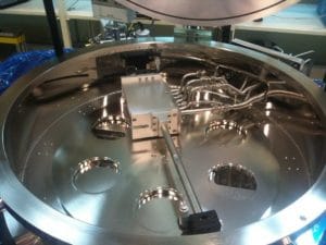
Atomic Layer Deposition (ALD)
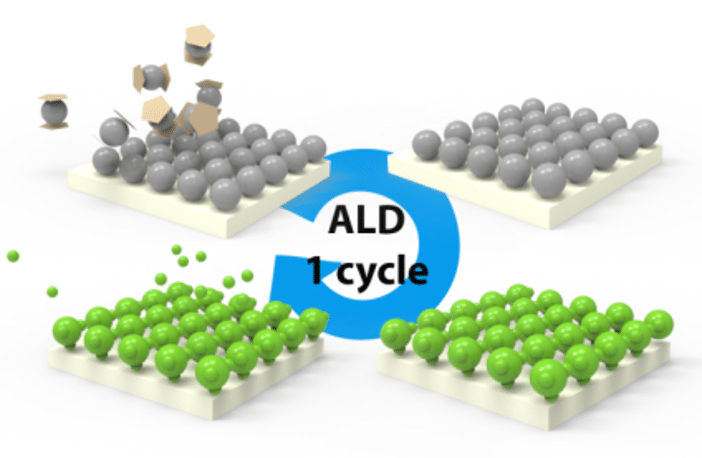
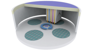
Figure. Schematic of atomic layer deposition
Given that the number of modern integrated devices is reducing, a deposition technique to produce high-quality films with atomic thickness controllability is necessary. One of the critical disadvantages of the existing methods (e.g., sputtering, chemical vapor deposition (CVD)) that cannot be applied to current fabrication of a sub-10 nm device fabrication is poor conformality. When the film is deposited on the high-aspect ratio substrate such as a trench or fin, the thickness on the top and bottom of the structure varies, resulting in the failure of the post-deposition process.
Unlike these deposition methods, ALD is one of the promising deposition technologies used in various fields that employ nanoscale fabrications including electronics, displays, energy applications, and functional coatings due to its unique deposition mechanism based on self-limiting surface-saturated reactions. When a precursor (or reactant) is exposed to the process chamber, the chemical species similarly react with the surface-adsorbed species. The residual species are purged out because no reaction sites are present on the surface.
The advantages of ALD such as excellent conformality and precise thickness control at the atomic scale over the conventional thin film deposition methods are its direct attractiveness for the nanoscale fabrication in a three-dimensional (3D) structure. Additionally, the cyclic exposure of the precursor and reactant in ALD reactions is another factor to enhance the atomic precision properties of thin films. For example, doping in films at the desired depth position is feasible by only adding dopant chemical exposure to normal ALD cycles without using expensive and complex tools, such as ion implantation. Additionally, metal alloys can be easily fabricated by combining two metal ALD processes. Considering that the amount of each metal can be controlled by the number of ALD cycle, a precise compositional control of alloy metals is also feasible, one of the advantages for the catalytic property maximization.
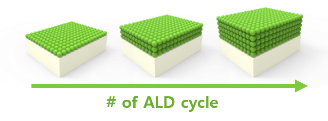
Thickness Controllability
ALD allows a sub-nanometer thickness control by modifying the number of the ALD cycles. The thickness of thin films can be controlled as a function of ALD cycles
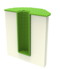
Excellent Conformality
Owing to the self-limiting surface saturation reaction of ALD, it enables excellent conformality on the high-aspect ratio substrate.
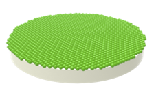
Large-area Uniformity
ALD ensures a large-area uniformity deposition owing to its unique saturated reaction. Thus, it is used for semiconductor or display fabrication.
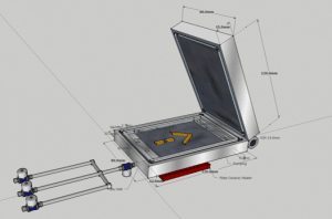
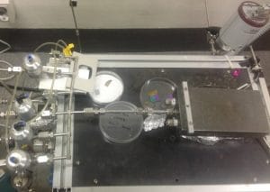
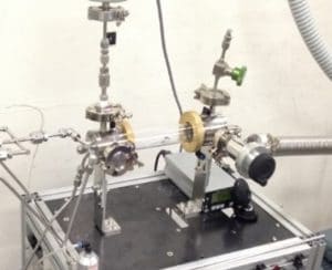
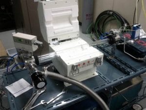
Design & Manufacture of Lab-scale ALD Chamber
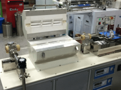
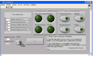
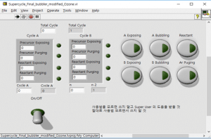
Regarding the ALD growth of thin film at low temperature, extremely small volume of chamber is required. Given that reactants (e.g., H2O) are easily adsorb on the chamber wall and purging it out is time consuming, the productivity of ALD at low process temperature drastically decreases. Therefore, ALD chamber with extremely small volume is designed and manufactured. To utilize this chamber for the ALD deposition, software for ALD process is developed with various functionalities by LabVIEW. To enhance the ALD productivity, a space-divided ALD tool with functional slit is also designed and manufactured.
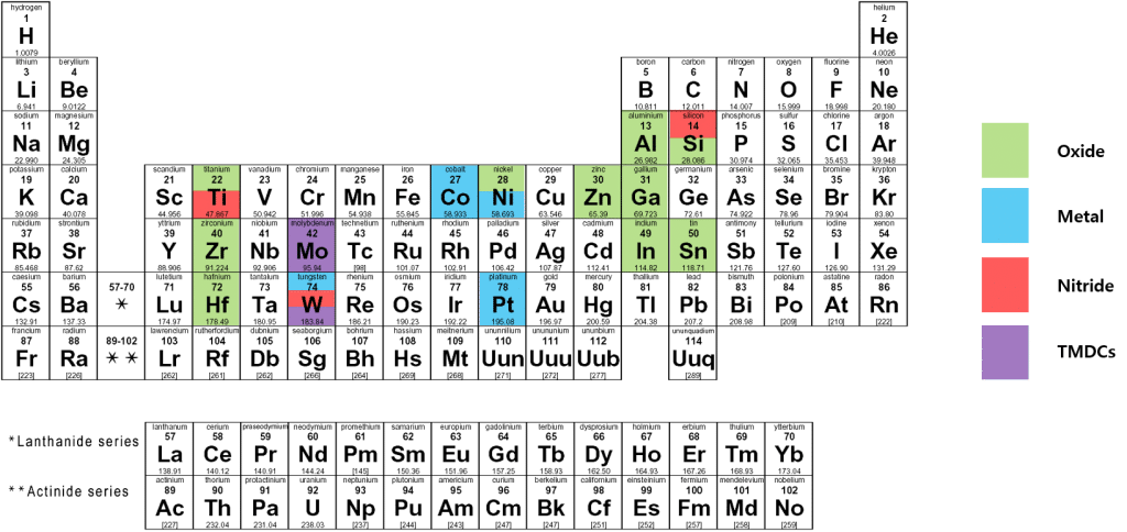
Deposition-available Materials by ALD (Experienced)
Copyrightⓒ 2018-2025. Taewook Nam. All right reserved.
